Applied Research and Development

Graphene, carbon, and process IP.

Structured research: hypotheses, lab capability, materials lock, simulation, fabrication pathway, characterization, IP. Prove function first. Scale only after the data holds.

Opportunities

Florida · Texas · Virginia

What we work on

Research lines, not product catalogs. Graphene electronics process, high-purity carbon interfaces, space thermal and semiconductor methods, and RF architecture. End use remains internal IP.

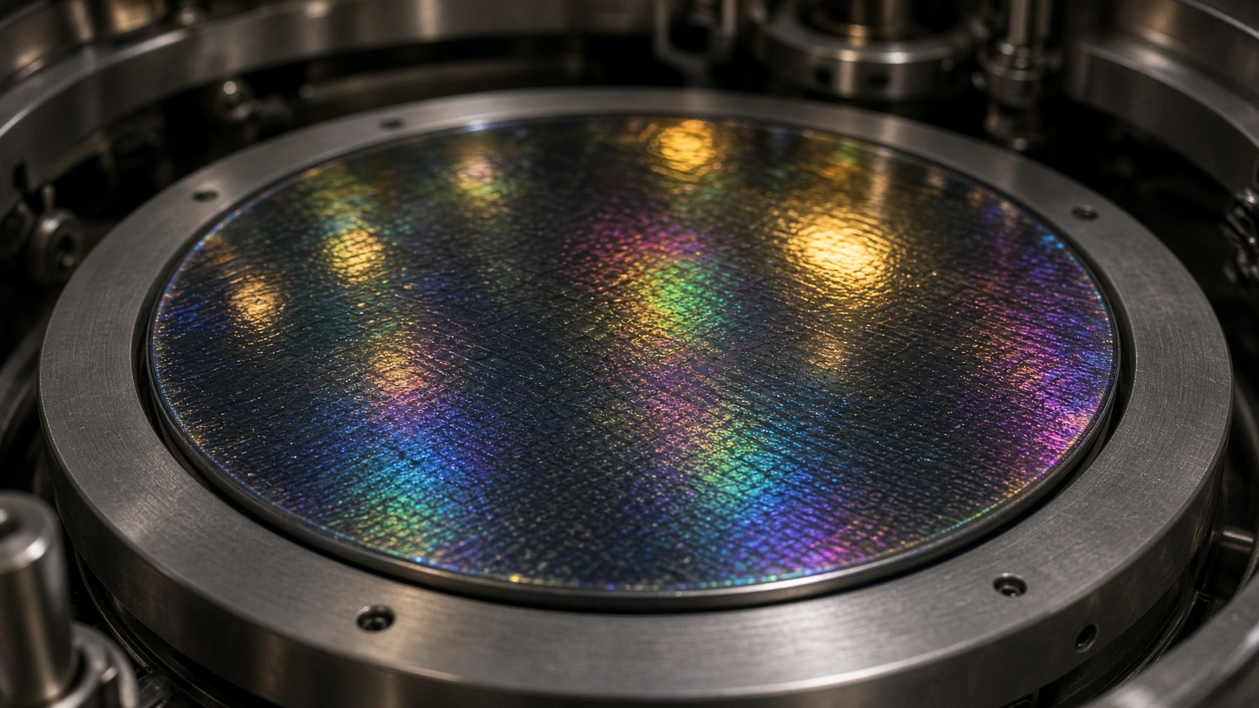
Graphene film on a silicon wafer in a process chamber

Graphene electronics process

Bandgap engineering for controlled switching. Architectural hypotheses on materials stack, channel geometry, and contacts. Fabrication pathway selection between academic labs and commercial foundries. CMOS-adjacent integration, packaging compatibility, and characterization for gain, noise, and temperature stability.

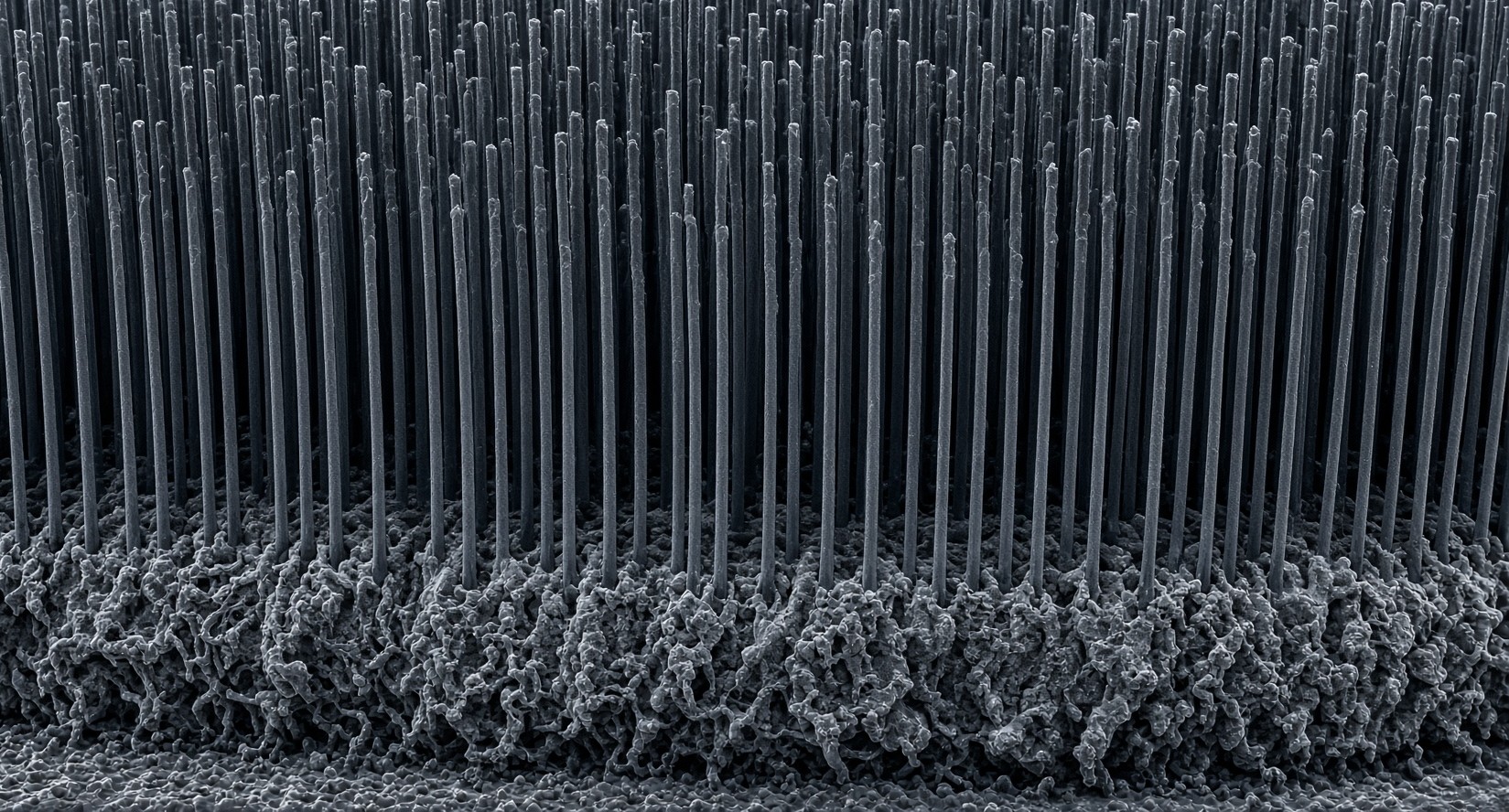
Aligned carbon nanotube forest under electron microscopy

High-purity graphene & interfaces

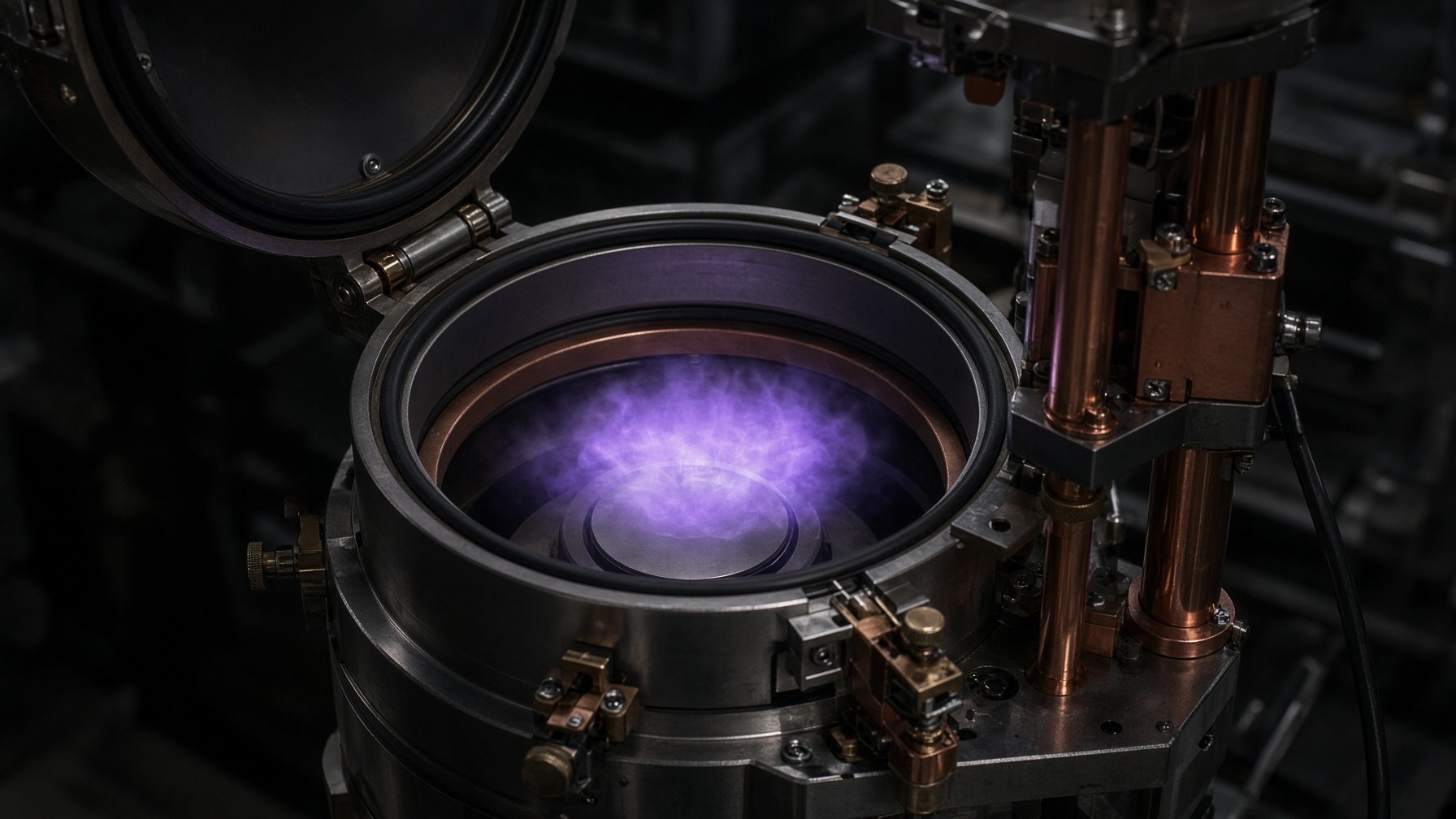
Graphene treated as a functional interface material — not an additive — for ionic and electronic conductivity, mechanical stability, and stress distribution. Purity qualification from 5N to 7N. Thermal-expansion production methods alongside CVD, plus carbon nanotubes and thin-film carbon.

Plasma-assisted thin-film carbon deposition in a vacuum chamber

Space thermal & semiconductor process

Radiative, conductive, and structural simulation. Surveys of space thermal architectures. Photoresist, RIE, and lattice-damage work for microgravity and high-energy particle environments. Graphene-on-copper thermal frames and ceramic–graphene insulation modeling.

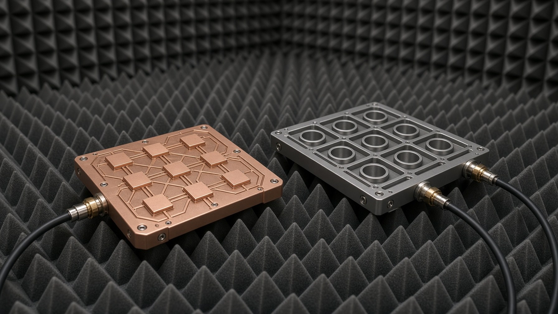
Precision copper and gallium alloy antenna arrays on a test bench

RF architecture research

Competitive landscape mapping. Frequency bands and beamforming targets. Narrowing of phased-array architecture. Copper and gallium antenna alloys, metamaterial response, and experimental validation — without treating the work as a finished radio product.

Method

How research is run

Prove functionality and reliability first. Integrate second. Scale materials and process only once performance is demonstrated. Technical truth-finding — not premature manufacturing.

01

Architectural hypotheses

Frame the physical problem: materials stack, geometry, contacts, interfaces. Lock what must be true before any scale discussion.

02

Lab & supplier assessment

Map who can actually run the process — internal labs, academic partners, foundries, and material suppliers. Capability first.

03

Landscape & scope

Competitive and technical landscape. Narrow frequency, geometry, or material scope so the program is testable.

04

Material candidate lock

Down-select graphene, carbon, electrolyte, electrode, or alloy candidates. Qualify purity, interfaces, and process compatibility.

05

Simulation

Thermal, charge, radiative, and structural models. Failure mechanisms into CAD-ready process behavior — including space and CMOS-adjacent cases.

06

Fabrication pathway

Academic versus commercial foundry. Wafer-scale intent only after the path is real. No premature manufacturing theater.

07

Characterization

Prototype fabrication and testing: mobility, gain, noise, temperature, optical phase, RF response. Honest assessment of what the data shows.

08

IP capture

Document process, models, and results as intellectual property. Pre-commercial. Scale only after performance is demonstrated.

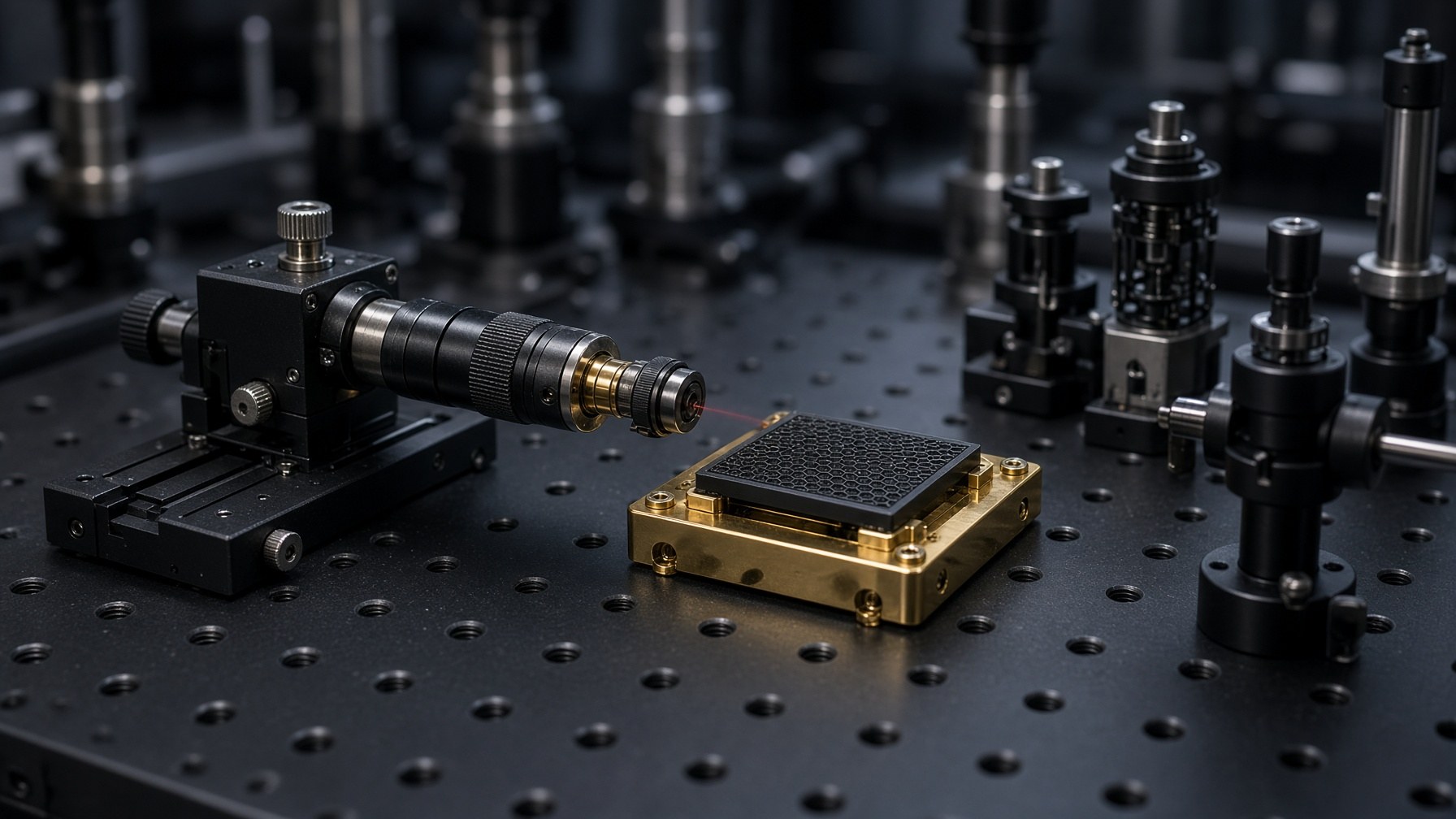
Graphene photonic chip on an optical research bench

Research

Graphene phase modulation

Graphene phase modulation alters light transmission and reception by electrostatically tuning the Fermi level of carbon layers. Voltage changes surface conductivity and the real part of the refractive index, shifting the phase of transmitted light with high efficiency and extreme bandwidth.

Electro-refraction

Voltage applied to graphene — often in double-layer capacitor setups — varies surface conductivity and refractive index without heavy optical loss.

Transparency regime

Raising the Fermi level past half the photon energy (Pauli blocking) keeps the material transparent while pure phase shifting occurs.

Interferometry

Graphene phase shifters sit inside Mach–Zehnder interferometers to convert phase shifts into high-contrast amplitude and phase data streams.

Electronics process

As silicon approaches physical limits, graphene offers electron mobility 10–100× higher, with thermal dissipation that supports denser layouts. Work includes bandgap engineering, prototype transistor structures, and wafer-scale process questions — packaging compatibility and foundry path, not a named device.

Research contexts

High-speed electronics, wireless and RF systems, sensing and instrumentation, photonics. Optical and electronic pathways on a shared platform. These are the problems we study. We do not publish the resulting assemblies.

Intellectual property

Patents and pre-commercial IP

We hold patents in graphene, carbon systems, and related process work. The portfolio is built to be developed — modeled, integrated, and carried toward pre-commercial use — not licensed as a brochure.

  1. 01

    Mobility of thermal and charge modeling and failure mechanism of CVD graphene in CMOS process integration

    Foundation for integrating graphene process behavior into CAD tools.

  2. 02

    Photoresist masking and exposure using high-energy beams in space and microgravity for semiconductor process migration to space

    Masking and exposure methods for semiconductor process work beyond Earth.

  3. 03

    RIE process adaptation in space and microgravity environments

    Reactive-ion etch process adaptation for microgravity fabrication.

  4. 04

    Lattice damage mechanism and preventive policy for IC process in space under high-energy particle exposure

    Damage modes and mitigation when integrated-circuit processes move to space.

  5. 05

    Thermal and charge modeling and failure mechanism of ceramic–graphene high thermal conductivity insulation

    3D modeling from micro-assembly through PBCA process.

  6. 06

    Graphene-on-copper sandwich frame thermal dynamics for HVAC on Earth and space-center orbit

    Thermal sandwich structures for terrestrial HVAC and orbital facilities.

Join AR&D

Applied Research and Development LLC is hiring in Florida, with work across Texas and Virginia. The bar is high. Open roles are listed below.

Data Analyst

Florida LLC · Full-time

Analyze experimental and materials data — including graphene process, thermal, and charge datasets — and support research and program decisions with rigorous analysis.

  • Strong quantitative and statistical skills
  • Experience with experimental or scientific datasets preferred
  • Clear communication of findings to technical teams

Program Analyst

Florida LLC · Full-time

Support planning, tracking, and execution of IP and pre-commercial research programs. Keep milestones, process work, and technical status clear across Florida, Texas, and Virginia.

  • Structured thinking and attention to detail
  • Comfort operating in technical environments
  • Ability to turn complexity into clear plans and status

Executive Operations Coordinator

Florida LLC · Full-time

Coordinate the executive office from Bonita Springs — calendar, travel, correspondence, and follow-through on decisions across research and operating locations.

  • Judgment and discretion with confidential work
  • Strong written communication
  • Ability to run an executive office without being asked twice

Administrative Assistant

Florida LLC · Full-time

Support the administrative office in Bonita Springs: scheduling, records, visitor and vendor coordination, and day-to-day operations of a Florida LLC.

  • Organized, precise, and reliable
  • Comfort with documents, calendars, and office systems
  • On-site presence in Bonita Springs

Research & Operations Associate

Florida LLC · Full-time

Bridge laboratory and program work — tracking experiments, materials, documentation, and operational needs so technical programs stay on schedule.

  • Comfort in both research and operations settings
  • Accurate documentation and follow-through
  • Willingness to work across Florida, Texas, and Virginia as needed

Material Scientist — Carbon

Florida LLC · Full-time

Lead and execute carbon materials work: graphene, carbon nanotubes, and thin-film carbon, including process, characterization, and pre-commercial development.

  • Deep background in carbon nanomaterials
  • Hands-on experimental and process judgment
  • Ability to turn results into IP-ready documentation

Material Scientist — Silicon

Florida LLC · Full-time

Work at the interface of silicon process, CMOS integration, and carbon-on-silicon questions — including space and microgravity process constraints.

  • Semiconductor process and silicon materials depth
  • Familiarity with CMOS integration challenges
  • Rigor in experimental design and failure analysis

Program Manager

Florida LLC · Full-time

Own multi-site research programs from scope through delivery. Coordinate scientists, analysts, and operations across Florida, Texas, and Virginia.

  • Proven program ownership in technical environments
  • Clear milestone discipline and risk reporting
  • Ability to manage IP-oriented, pre-commercial work

Send a résumé and a short note on relevant work to careers@appliedresearchanddevelopment.com.

Contact

Talent inquiries and general contact.

Administrative office

26381 South Tamiami Trail
Suite 300
Bonita Springs, FL 34134

Florida LLC. Offices in Texas and Virginia.

General: contact@appliedresearchanddevelopment.com

Careers: careers@appliedresearchanddevelopment.com